


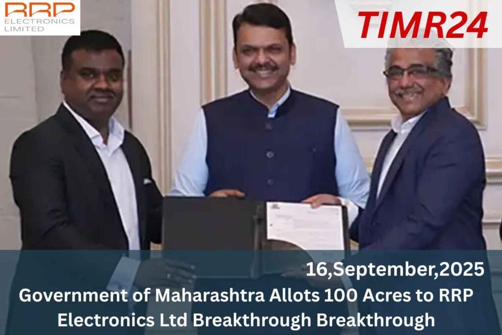
RRP Electronics has secured 100 acres in Navi Mumbai for a semiconductor fab, following a Letter of Comfort from Chief Minister Devendra Fadnavis. The move positions Maharashtra at the center of India’s Semiconductor Mission roadmap, aiming to accelerate industrial growth, create employment opportunities, strengthen local supply chains, and reinforce Maharashtra’s leadership as a hub for high-technology manufacturing. This acquisition marks a significant step in RRP’s growth journey, as it is one of the region’s largest and most advanced fab facilities In a monumental stride towards fortifying India’s position in the global semiconductor landscape, the Government of Maharashtra has allocated.
100 acres of land in Navi Mumbai to RRP Electronics Ltd. This strategic move is poised to catalyze the nation’s ambitions of achieving self-reliance in semiconductor production, aligning seamlessly with the objectives of India’s Semiconductor Mission The 100-acre land parcel, situated in Navi Mumbai, is earmarked for the establishment of a state-of-the-art semiconductor fabrication facility. This facility is (REITs) set to have a production capacity of 125,000 wafers per month, positioning it among the largest and most advanced semiconductor fabs in the region. The project’s estimated cost stands at ₹12,035 crore, underscoring its scale and the substantial investment in India’s technological infrastructure.
RRP Electronics Ltd: A Visionary Endeavor
RRP Electronics Ltd., a cutting-edge Semiconductor Company, is spearheading this initiative. Backed by cricket legend Sachin Tendulkar, the company has been at the forefront of semiconductor packaging technologies. The establishment of this fabrication facility marks a significant expansion of RRP Electronics’ capabilities, transitioning from packaging to full-fledged semiconductor manufacturing. This move is expected to bolster India’s domestic production of semiconductors, reducing reliance on imports and enhancing the resilience of the supply chain The Maharashtra government’s proactive approach in facilitating this project is evident through the issuance of a.
Letter of Comfort to RRP Electronics. Chief Minister Devendra Fadnavis emphasized the state’s commitment to providing necessary support in infrastructure, policy facilitation, and skill development to ensure the success of this initiative. Such backing is crucial in creating an enabling environment for high-tech manufacturing ventures This development aligns with India’s broader Semiconductor Mission, which aims to establish a robust semiconductor manufacturing ecosystem within the country. By attracting investments in semiconductor fabrication, India seeks to mitigate the challenges posed by global supply chain disruptions and to position itself as a significant player in the Semiconductor Industry.
The establishment of the semiconductor fab is expected to generate substantial employment opportunities, both directly and indirectly. Skilled labor will be required for the operation and maintenance of the facility, while ancillary industries such as logistics, equipment supply, and research and development will also experience growth. This job creation is anticipated to have a positive ripple effect on the local economy in Navi Mumbai and the broader Maharashtra region The proposed semiconductor fab will incorporate cutting-edge technologies in semiconductor manufacturing, including advanced photolithography, etching, and deposition techniques.
Infrastructure and Connectivity Enhancements
The facility’s design will adhere to international standards, ensuring the production of high-quality semiconductors that meet the demands of various industries, including electronics, automotive, telecommunications, and consumer goods The location in Navi Mumbai offers strategic advantages in terms of infrastructure and connectivity. Proximity to major ports, airports, and transportation networks will facilitate the efficient movement of raw materials and finished products. Additionally, the region’s existing industrial ecosystem provides a conducive environment for collaboration and innovation among technology companies. In line with global trends towards sustainable.
Manufacturing practices, the semiconductor fab is expected to incorporate environmentally friendly technologies. This includes the adoption of energy-efficient processes, waste minimization strategies, and water recycling systems. Such measures will contribute to reducing the environmental footprint of semiconductor manufacturing activities Looking ahead, RRP Electronics Ltd. envisions expanding its operations beyond the initial phase of the semiconductor fab. Plans include the development of research and development centers, training institutes, and collaboration with academic institutions to foster innovation and skill development in semiconductor technologies.
These initiatives will further strengthen India’s position in the global semiconductor value chain The allocation of 100 acres to RRP Electronics Ltd. by the Government of Maharashtra is a landmark decision that underscores the state’s commitment to advancing India’s semiconductor manufacturing capabilities. This initiative not only promises to (RRP) enhance technological self-reliance but also to stimulate economic growth, create employment opportunities, and foster innovation. As the project progresses, it is expected to serve as a model for future endeavours in high-tech manufacturing within the country.